GaNのエピタキシアル ウエファー
(69)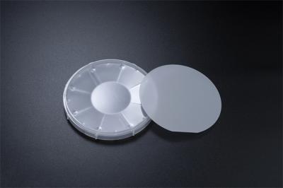
4 インチ P 型 Mg ドープ GaN オン サファイア ウエハー SSP 抵抗率~10Ω Cm LED レーザー PIN エピタキシャル ウエハー
価格: Negotiable
MOQ: Negotiable
納期: 3-4 week days
ブランド: GaNova
ハイライト:LED Laser PIN Epitaxial Wafer
サファイアウェーハ上の4インチP型MgドープGaN SSP抵抗率〜10Ωcm LED、レーザー、PINエピタキシャルウェーハ
p 型 Mg ドープ GaN の電気特性は、可変温度ホール効果測定によって調査されます。Mg ドーピング濃度の範囲を持つサンプルは、有機金属化学気相堆積によって準備されました。
ドーパント密度がデバイス アプリケーションで通常使用される高い値に増加すると、多くの現象が観察されます。実効アクセプター エネルギー深度が 190 meV から 112 meV に減少し、低温での不純物伝導がより顕著になり、補償比が増加し、価電子帯の移動度が急激に低下します。
... もっと見る
今コンタクトしてください
FeはGaNの基質の抵抗を> 10 ⁶ Ω添加した·Cm RF装置
価格: Negotiable
MOQ: Negotiable
納期: 3-4 week days
ブランド: GaNova
ハイライト:ISO GaN Substrates, gan semiconductor wafer, Fe Doped GaN Substrates
2inch C-face Fe-doped SI-type free-standing GaN single crystal substrate Resistivity > 106 Ω·cm RF devices The achieved breakdown voltage of the Fe-doped GaN epitaxial layer can be as high as 2457 V, which is attributed to the Fe-doped GaN epitaxial layer with higher resistance, which can sustain... もっと見る
今コンタクトしてください
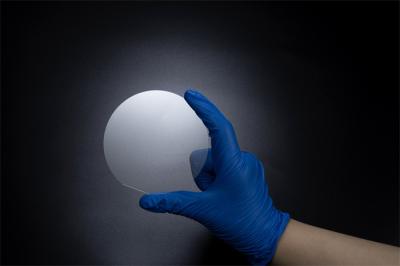
サファイアSSPの平らなサファイアの675um 4インチ青いLED GaNのエピタキシアル ウエファーへの625um
価格: Negotiable
MOQ: Negotiable
納期: 3-4 week days
ブランド: GaNova
ハイライト:625um GaN Epitaxial Wafer, SSP gan on sapphire wafers, 675um GaN Epitaxial Wafer
Substrate Thickness 650 ± 25 μm 4 Inch Blue LED GaN Epitaxial Wafer On Sapphire SSP Flat Sapphire 4 inch Blue LED GaN epitaxial wafer on sapphire SSP For example, GaN is the substrate which makes violet (405 nm) laser diodes possible, without use of nonlinear optical frequency-doubling. Its sensitiv... もっと見る
今コンタクトしてください

2インチ緑色LEDガナオンシリコン・ウェーバー 寸法520±10nm
価格: Negotiable
MOQ: Negotiable
納期: 3-4 week days
ブランド: GaNova
ハイライト:シリコン・ウェーバーの2インチGAN, 緑色LED GaN シリコン・ウェーバー, シリコン・ウェーバー上の520nmのガナ
シリコンウエハー上の2インチ緑色LED GaN
概要
窒化ガリウム (GaN) は、パワー エレクトロニクスの世界全体に革新的な変化をもたらしています。何十年もの間、シリコンベースの MOSFET (金属酸化膜半導体電界効果トランジスタ) は、エネルギーを電力に変換するのに役立つ現代社会の不可欠な部分でした。
敵対的生成ネットワーク (GAN) は、2 つのニューラル ネットワークを使用するアルゴリズム アーキテクチャであり、実際のデータを渡すことができるデータの新しい合成インスタンスを生成するために、一方を他方 (したがって「敵対的ネットワーク」) と対戦させます。それらは、画像生... もっと見る
今コンタクトしてください
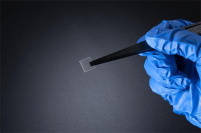
10 X 10.5 mm2 C 顔 無剤 N タイプ 立立体 単結晶基板
価格: Negotiable
MOQ: Negotiable
納期: 3-4 week days
ブランド: GaNova
ハイライト:塩基配合剤が使用されていないGAN単結晶基板, 支えがないGaNの単結晶の基質, N型GAN単結結晶基板
10*10.5mmの²のC表面Un-doped nタイプの支えがないGaNの単結晶の基質の抵抗 < 0="">
概観
低い転位密度(105 /cm2の順序で)および周期的な欠陥無しのユニフォームの表面が付いている優れた質のGaNの水晶基質。GaNのこれらの良質の水晶に使用可能な区域がの90%以上ある。
従って私達は工場から直接販売し、GaNの良質の水晶基質のための市場の最もよい価格を提供してもいい。
10 x 10.5 mm2支えがないGaNの基質
項目
GaN FSC U S10... もっと見る
今コンタクトしてください

10*10.5mm2 C-Face Fe-Doped SI型自由立体GaNシングルクリスタル基板 マクロデフェクト密度 0cm−2 TTV ≤ 10μm 抵抗 106 Ω·Cm RFデバイス
価格: Negotiable
MOQ: Negotiable
納期: 3-4 week days
ブランド: GaNova
ハイライト:GaNの単結晶の基質, 10*10.5mm2 GaN シングルクリスタル基板
10*10.5mm2 C表面はSIタイプの支えがないGaNの単結晶の基質の抵抗を> 106 Ω Fe添加した·cm RF装置ウエファー
概観
従って私達は工場から直接販売し、GaNの良質の水晶基質のための市場の最もよい価格を提供してもいい。世界からの顧客はGaNの水晶基質の優先する製造者として私達の供給を信頼した。
ガリウム窒化物、かGaNは、充電器で半導体に使用し始めている材料である。90年代に始まるLEDsを作ることを使用しまた衛星の太陽電池の配列のための普及した材料である。充電器に関してはGaNについての主な事柄はより少ない熱を作り出すことである。
... もっと見る
今コンタクトしてください
10 × 10.5 mm2 自由に立つGaN基板 - 10 μm ≤ BOW ≤ 10 μm
価格: Negotiable
MOQ: Negotiable
納期: 3-4 week days
ブランド: GaNova
ハイライト:GaNの自由で永続的な基質, 10 × 10.5 mm2 ガナンの基板
10*10.5mm² C面 アンドープn型自立GaN単結晶基板 抵抗率 < 0.1Ω・cm パワーデバイス/レーザー
アプリケーション
レーザーダイオード:紫LD、青LD、緑LDパワーエレクトロニクスデバイス、高周波電子デバイス
10 年以上の GaAs 基板のウェーハ製造技術の経験が GaN 基板の製造に適用されています。GaN 基板は、損傷がなく、非常に平坦 (Rms < 0.2 nm)、制御された表面配向、制御された原子ステップ表面を備えています。エピタキシャル成長に適した表面品質を実現しています。
... もっと見る
今コンタクトしてください

TTV ≤ 10μm A-Face 無ドーピング N型自由立体 GaN シングルクリスタル基板 抵抗性 0.1 Ω·cm 電力装置/レーザー W
価格: Negotiable
MOQ: Negotiable
納期: 3-4 week days
ブランド: GaNova
ハイライト:レーザー W GaN シングルクリスタル基板, 電力装置 GaN シングルクリスタル基板, 自由に立つGaN単結晶基板
5*10mm2表面Un-doped nタイプの支えがないGaNの単結晶の基質の抵抗 < 0="">
概観ガリウム窒化物(GaN)は非常に堅い、機械的に安定した広いbandgapの半導体である。より高い故障の強さによって、より速く切り替え速度、より高い熱伝導性はオン抵抗、GaNに基づいて力装置を下げるためにかなりケイ素 ベースの装置に優り。ノースカロライナ州立大学およびパデュー大学からの研究者は半導体材料ガリウム窒化物(GaN)が無毒で、ヒト細胞–いろいろ生物医学的なインプラント技術の材料の使用へドアを開けることと互換性があることを示した。
表面支... もっと見る
今コンタクトしてください

350 ± 25μm 厚さ 塩基配合されていないN型自由立体GANシングルクリスタル基板 TTV ≤ 10μm 抵抗度は0.1 Ω·cm
価格: Negotiable
MOQ: Negotiable
納期: 3-4 week days
ブランド: GaNova
ハイライト:10μm GaN シングルクリスタル基板, GaNの単結晶の基質
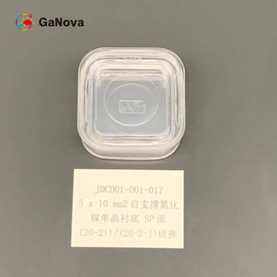
5*10mm2 SP表面(20-21)/(20-2-1) Un-doped nタイプの支えがないGaNの単結晶の基質の抵抗 < 0="">
概観ガリウム窒化物(GaN)の基質は良質のsingle-crystal基質である。それは元のHVPE方法および最初に長年にわたり開発されたウエファーの加工技術となされる。特徴は高い結晶、よい均等性および優秀な表面質である。
GaNは広い応用範囲を渡るかなり改善された性能を提供する機能のために重要性で慣習的なケイ素の技術と比較するとその性能を提供するのに必要とされるエネルギーおよび物理的な空間を減らしている間育っている。
... もっと見る
今コンタクトしてください
5*10mm2 SP-Face 10-11 無ドーピング N型自由立 GaN単結晶基板 0.1 Ω·cm 電源装置に対する耐性
価格: Negotiable
MOQ: Negotiable
納期: 3-4 week days
ブランド: GaNova
ハイライト:0.1 Ω·cm GaN シングルクリスタル基板, 5*10mm2 GaN シングルクリスタル基板
5*10.5mm2 SP表面(10-11) Un-doped nタイプの支えがないGaNの単結晶の基質の抵抗 < 0="">
生成的な敵対的なネットワーク(GANs)は2つのニューラル・ネットワークを使用する実質データのために渡ることができるデータの新しく、総合的な例を発生させるために他に対して1つを凹めるアルゴリズムの建築(こうして「敵対的な」)である。それらはイメージの生成、ビデオ生成および声の生成で広く使用される。
(10- 11) GaNの支えがない基質に直面しなさい
項目
GaN FS SPU S
... もっと見る
今コンタクトしてください
5x10mm2 SP-Face 10-11 無ドーピング N型自由立体GANシングルクリスタル基板 TTV ≤ 10μm 抵抗力0.05 Ω·cm
価格: Negotiable
MOQ: Negotiable
納期: 3-4 week days
ブランド: GaNova
ハイライト:支えがないGaNの単結晶の基質, 5x10mm2 GaN シングルクリスタル基板
5*10mm2 SP表面(10-11) Un-doped nタイプの支えがないGaNの単結晶の基質の抵抗 < 0="">
概観GaNにケイ素上の多くの深刻な利点があり、有効、より速いに動力を与え、もっと回復特徴をよくすることである。但し、GaNは優秀な選択のようにようであるかもしれないがそれはすべての適用のケイ素をしばらく取り替えない。
Semi-insulating (SI) GaNは光学音量子の第2倍音の吸収が行われる0.36のµm to~7のµmから透明であると知られている。
(10- 11) GaNの支えがない基質に直面しなさい
... もっと見る
今コンタクトしてください
マクロデフェクト密度 0cm−2 無ドーピング式 SI型 無線通信機器のための自由立体GANシングルクリスタル基板 5*10mm2 M面
価格: Negotiable
MOQ: Negotiable
納期: 3-4 week days
ブランド: GaNova
ハイライト:RFデバイス GaN シングルクリスタル基板, 5*10mm2 GaN シングルクリスタル基板, 自由に立つGaN単結晶基板
5*10mm2 M表面Un-doped SIタイプの支えがないGaNの単結晶の基質の抵抗> 106 Ω·cm RF装置ウエファー
概観Epiの薄いウエファーはリーディング エッジMOS装置のために一般的である。厚いEpiがか多層のエピタキシアル ウエファーは装置のために電力を制御するのに主に使用されエネルギー消費の効率の改善に貢献している。
ガリウム窒化物(GaN)の基質は良質のsingle-crystal基質である。それは元のHVPE方法および最初に長年にわたり開発されたウエファーの加工技術となされる。特徴は高い結晶、よい均等性および優秀な表面質である。
... もっと見る
今コンタクトしてください

SP-Face 11-12 無ドーピング N型自由立体GAN単結晶基板 抵抗力0.05 Ω·cm マクロ欠陥密度0cm−2
価格: Negotiable
MOQ: Negotiable
納期: 3-4 week days
ブランド: GaNova
ハイライト:0.05 Ω·cm GaN シングルクリスタル基板, 塩基配合剤が使用されていないGAN単結晶基板
5×10mm2SP 面 (11-12) アンドープ n 型自立 GaN 単結晶基板 抵抗率 < 0.05 Ω・cm パワーデバイス/レーザーウェーハ
概要GaNトランジスタはシリコン・トランジスタよりも高速にターンオンできるため、この遷移による損失を減らすことができます。GaN がスイッチング損失を低減するもう 1 つの方法は、ボディ ダイオードがないことです。
GaNは、従来のシリコン技術と比較して、その性能を実現するために必要なエネルギーと物理的スペースを削減しながら、幅広いアプリケーションにわたって大幅に改善された性能を提供できるため、重要性が増しています。
... もっと見る
今コンタクトしてください

電力装置 5x10mm2 無ドープ N型自由立体GANシングルクリスタル基板 抵抗力0.1 Ω·cmとBOW 10μm以内
価格: Negotiable
MOQ: Negotiable
納期: 3-4 week days
ブランド: GaNova
ハイライト:0.1 Ω·cm GaN シングルクリスタル基板, 10μm GaN シングルクリスタル基板, 5x10mm2 GaN シングルクリスタル基板
5*10mm2 SP表面(11-12) Un-doped nタイプの支えがないGaNの単結晶の基質の抵抗 < 0="">
概観90年代以来、ずっとそれは発光ダイオード(LED)で一般に使用されている。ガリウム窒化物はBlu-rayでディスク読書に使用する青いライトを放つ。さらに、ガリウム窒化物は半導体力装置、RFの部品、レーザーおよびphotonicsで使用される。将来、私達はセンサー技術のGaNを見る。
(11- 22) GaNの支えがない基質に直面しなさい
項目
GaN FS SPU S
... もっと見る
今コンタクトしてください
5*10mm2 SP-Face 無ドーピング N型自由立体ガナ単結基質 20-21 / 20-2-1 10mm2 抵抗力 0.05 Ω·cm
価格: Negotiable
MOQ: Negotiable
納期: 3-4 week days
ブランド: GaNova
ハイライト:0.05 Ω·cm GaN シングルクリスタル基板, 10mm2 GaN シングルクリスタル基板, 20〜21 GaN シングルクリスタル基板
5*10mm2 SP表面(20-21)/(20-2-1) Un-doped nタイプの支えがないGaNの単結晶の基質の抵抗 < 0="">
概観生成的な敵対的なネットワーク(GAN)に2部がある:発電機はもっともらしいデータを発生させることを学ぶ。発生させた例は識別器のための否定的な訓練の例になる。識別器は実質データと発電機の擬似データを区別することを学ぶ。
(20- 21)/(20- 2- 1) GaNの支えがない基質に直面しなさい
項目
GaN FS SPU S
GaN FS SPN S
GaN FS SP... もっと見る
今コンタクトしてください
シリコンの薄片20nmContactの層の次元520±10nm 2inch緑主導のGaN
価格: Negotiable
MOQ: Negotiable
納期: 3-4 week days
ブランド: GaNova
ハイライト:20nm GaN On Silicon Wafer, 520±10nm GaN On Silicon Wafer
シリコンの薄片の2inch緑主導のGaN
概観
ガリウム窒化物(GaN)はパワー エレクトロニクスの世界中の革新的な転位を作成している。長年に渡って、ケイ素 ベースのMOSFETs (金属酸化膜半導体の電界効果トランジスタ)は動力を与えるために改宗者エネルギーを助ける毎日の現代世界のずっと重要部分である。
生成的な敵対的なネットワーク(GANs)は2つのニューラル・ネットワークを使用する実質データのために渡ることができるデータの新しく、総合的な例を発生させるために他に対して1つを凹めるアルゴリズムの建築(こうして「敵対的な」)である。それらはイメージの生成、ビデオ生成および声の生... もっと見る
今コンタクトしてください

シリコンの薄片のLongueurのD'Ondeレーザー455±10nmの2inch青主導のGaN
価格: Negotiable
MOQ: Negotiable
納期: 3-4 week days
ブランド: GaNova
ハイライト:455±10nm GaN On Silicon Wafer
シリコンの薄片の2inch青主導のGaN
ガリウム窒化物は高い発電、高周波半導体の塗布に使用する半導体技術である。ガリウム窒化物はそれをさまざまな高い発電の部品のためのGaAsそしてケイ素よりよくさせる複数の特徴を表わす。これらの特徴はより高い絶縁破壊電圧およびよりよい電気抵抗を含んでいる。
ケイ素の2inch GaN青いレーザー
項目
Siの(111の)基質
Al (Ga) Nの緩衝
uGaN
nGaN
AlGaN
InGaN
MQW
(1-3組)
... もっと見る
今コンタクトしてください

2 インチ C 面 Fe ドープ SI タイプ自立型 GaN 単結晶基板 抵抗率 > 10⁶ Ω·cm RF デバイス
価格: Negotiable
MOQ: Negotiable
納期: 3-4 week days
ブランド: Nanowin
ハイライト:2inch GaN Single Crystal Substrate, Resistivity GaN Single Crystal Substrate
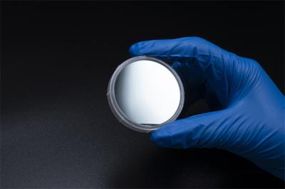
2inch C面FeドープSI型自立GaN単結晶基板 抵抗率>106Ω・cm RFデバイス
概要
窒化ガリウム (GaN) エピタキシャルウェーハ (エピウェーハ)。シリコン基板、サファイア基板、炭化ケイ素 (SiC) 基板などのさまざまな基板上の GaN 高電子移動度トランジスタ (HEMT) ウェーハ。当社は、RF およびパワー アプリケーション向けに GaN on SiC ウエハーを提供しています。
2インチ自立型U-GaN/SI-GaN基板
エクセレントレベル(S)
... もっと見る
今コンタクトしてください

4インチによってMg添加されるGaN/サファイアの基質SSP Resistivity~10Ω cm LEDレーザーPINのエピタキシアル ウエファー
価格: Negotiable
MOQ: Negotiable
納期: 3-4 week days
ブランド: GaNova
ハイライト:LED Laser GaN Epitaxial Wafer
サファイアのウエファーSSP resistivity~10Ω cm LED、レーザーのPINのエピタキシアル ウエファーの4インチPタイプのMg添加されたGaN
なぜGaNのウエファーを使用しなさいか。
サファイアのガリウム窒化物は無線エネルギー拡大のための理想的な材料である。それは高温でより高い絶縁破壊電圧およびよりよい性能を含むケイ素上のいくつかの利点を、提供する。
GaNは90年代以来の明るい発光ダイオードで一般的な二進III/Vの直接bandgapの半導体である。混合物はウルツ鉱の結晶構造がある非常に堅い材料である。3.4 eVのその広いバンド ギャップはそれを適用の... もっと見る
今コンタクトしてください
4 インチ N 型 UID ドープ GaN オン サファイア ウェーハ SSP 抵抗率>0.5 Ω cm LED、レーザー、PIN エピタキシャル ウェーハ
価格: Negotiable
MOQ: Negotiable
納期: 3-4 week days
ブランド: GaNova
ハイライト:PIN GaN On Sapphire Wafer, 4 Inch GaN On Sapphire Wafer
4 インチ N 型 UID ドープ GaN on サファイア ウェーハ SSP 抵抗率>0.5 Ω cm LED、レーザー、PIN エピタキシャル ウェーハ
たとえば、GaN は、非線形光周波数倍増を使用せずに、紫色 (405 nm) レーザー ダイオードを可能にする基板です。電離放射線に対する感度が低いため (他の III 族窒化物と同様)、衛星用の太陽電池アレイに適した材料となっています。デバイスは放射線環境で安定性を示しているため、軍事および宇宙アプリケーションも恩恵を受ける可能性があります。
4インチアンドープGaN/サファイア基板
... もっと見る
今コンタクトしてください