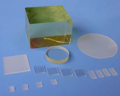
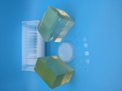
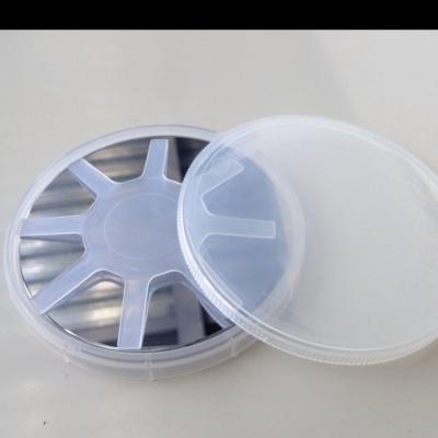
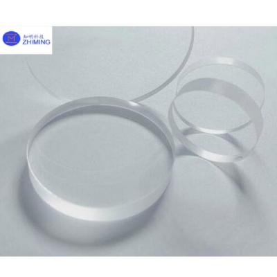
リン化インジウムのウエファー
(33)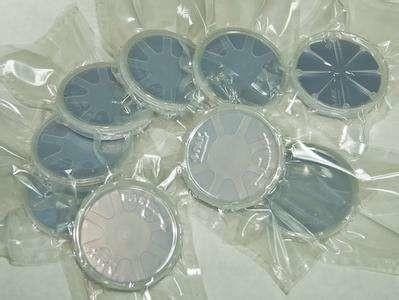
黒いリン化インジウムのウエファー、LDの適用のための半導体ウエハー
価格: by case
MOQ: 5pcs
納期: 1-4weeks
ブランド: zmkj
ハイライト:mgoの基質, ギャップのウエファー
LDの適用のための2inch 3inch 4inch INP基質、半導体ウエハー、INPウエファー、単結晶のウエファー
INPは導入します
INP単結晶
tCZの成長(Czochralski変更された方法)が種から始まってホウ素の酸化物の液体のencapsulantによって単結晶を引っ張るのに使用されています。添加物(Fe、S、SnまたはZn)はpolycrystalと共にるつぼに加えられます。高圧は部屋の中でリン化インジウムの分解を防ぐために適用されます。私達は十分にstoechiometric、高い純度および低い転位密度INP単結晶をもたらす... もっと見る
➤ 訪問 Webサイト
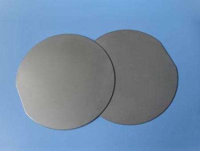
GEの光学版のリン化インジウムのウエファーの優秀な半導体材料
価格: by case
MOQ: 3pcs
納期: 1-4weeks
ブランド: zmkj
ハイライト:mgoの基質, ギャップのウエファー
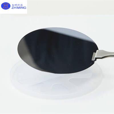
ゲルマニウムの単結晶のウエファー、GEの光学版
ゲルマニウムの基質
適用:半導体デバイス、赤外線光線の光学装置、太陽電池の沈降材料の生産で使用されるゲルマニウムのウエファー。
主要な特性の言葉
生産方法
Czochralski方法(CZ)
結晶構造
立方体
格子定数
a=5.65754Å
密度
5.323g/cm3
融点
937.4℃
添加された材料
どれもまたは添加されたSb添加しませんでした
添加されるインジウムかガリウム
タイプ
... もっと見る
➤ 訪問 Webサイト
GEレンズの半導体の基質INPインジウム ガリウム リン化物のウエファー
価格: by case
MOQ: 3pcs
納期: 1-4weeks
ブランド: zmkj
ハイライト:GEレンズのリン化インジウムのウエファー, 半導体の基質のリン化インジウムのウエファー, INP GEの単結晶
4inch 6inchのゲルマニウムの単結晶GEの基質のウエファー、カスタマイズされたGEの光学レンズ
ゲルマニウムの基質
適用:半導体デバイス、赤外線光線の光学装置、太陽電池の沈降材料の生産で使用されるゲルマニウムのウエファー。
主要な特性の言葉
生産方法
Czochralski方法(CZ)
結晶構造
立方体
格子定数
a=5.65754Å
密度
5.323g/cm3
融点
937.4℃
添加された材料
どれもまたは添加されたSb添加しなかった... もっと見る
➤ 訪問 Webサイト
4インチのLDの半導体レーザーのためのSemi-Insulatingリン化インジウムINPウエファー
価格: by case
MOQ: 10pcs
納期: 3-4weeks
ブランド: zmkj
ハイライト:INPウエファー, mgoの基質
4inch LDの半導体レーザーのためのSemi-Insulatingリン化インジウムINPウエファー、半導体ウエハー、3inch INPウエファー、LDの適用のための単結晶wafer2inch 3inch 4inch INP基質、半導体ウエハー、INPウエファー、単結晶のウエファー
INPは導入する
INP単結晶
成長(Czochralski変... もっと見る
➤ 訪問 Webサイト
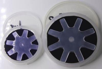
3.58密度Mgoの基質/Mgoのウエファーの酸化マグネシウムの水晶の基質
価格: by case
MOQ: 10pcs
納期: 1-4weeks
ブランド: zmkj
ハイライト:INPウエファー, ギャップのウエファー
MgOの基質、10X10mm MgOのウエファー、半導体ウエハー、酸化マグネシウムの(MgO)の水晶基質、水晶の製造者MgOのウエファー5x5mm製品の説明:酸化マグネシウム(MgO)はモノクリスタル基質のために優秀ferroelectric薄膜の生産で広く利用されていますです、彼は磁気フィルムの、光学フィルムおよび高温超伝導の薄膜、等マイクロウェーブ バンド比誘電率に損失が小さいある、およびそれです現在の企業、単一水晶の基質の重要な高温超伝導の薄膜ので基質(2インチの直径およびより大きい)の大きい区域を得てもいく。高温超伝導のマイクロウェーブ フィルターおよび他の装置に必要な移動体通信装置を... もっと見る
➤ 訪問 Webサイト
ゲルマニウムの単結晶INPウエファーの半導体の基質
価格: by case
MOQ: 3pcs
納期: 1-4weeks
ブランド: zmkj
ハイライト:INPウエファーの半導体の基質, 半導体のゲルマニウムINPウエファー, ゲルマニウムの単結晶の基質
4inch 6inchのゲルマニウムの単結晶GEの基質のウエファー、カスタマイズされたGEの光学レンズ
ゲルマニウムの基質
適用:半導体デバイス、赤外線光線の光学装置、太陽電池の沈降材料の生産で使用されるゲルマニウムのウエファー。
主要な特性の言葉
生産方法
Czochralski方法(CZ)
結晶構造
立方体
格子定数
a=5.65754Å
密度
5.323g/cm3
融点
937.4℃
添加された材料
どれもまたは添加されたSb添加しなかった... もっと見る
➤ 訪問 Webサイト

半絶縁の2インチ50mm Nのタイプ模造INPリン化インジウムのウエファー
価格: by case
MOQ: 3pcs
納期: 3-4weeks
ブランド: zmkj
ハイライト:50mmのリン化インジウムのウエファー, 半絶縁のリン化インジウムのウエファー, nのタイプINPウエファー
2inch dia50.8mmのnタイプの模造の主な等級INPリン化インジウムのウエファー
4inch LDの半導体レーザーのためのSemi-Insulatingリン化インジウムINPウエファー、半導体ウエハー、3inch INPウエファー、LDの適用のための単結晶wafer2inch 3inch 4inch INP基質、半導体ウエハー、INPウエファー、単結晶のウエファー
INPは導入する ... もっと見る
➤ 訪問 Webサイト
高い屈折するDSP表面GEのゲルマニウムのウエファー
価格: by case
MOQ: 3pcs
納期: 1-4weeks
ブランド: zmkj
ハイライト:DSPの表面のゲルマニウムのウエファー, 高い屈折するゲルマニウムのウエファー, DSP表面GEのウエファー
2inch 4inch 6inch NのタイプPのタイプはゲルマニウムの単結晶のウエファーを添加した、
ゲルマニウムの単結晶の光学版
GEのウエファー/GEの窓
ゲルマニウム(GE)は高性能8-12 um波長バンドの赤外線イメージ投射 システムのための優先するレンズおよび窓材料である。その高いr.i.は最低の表面の湾曲のために低い電力イメージ投射 システムのためのGEの理想を作る。色収差は小さく、頻繁に訂正のための必要性を除去する。
概要の特性
一般的な特性は構成する
、= 5.6754 Å立方
密度:5... もっと見る
➤ 訪問 Webサイト
GE光学INPウエファー、半導体デバイスのリン化インジウムのウエファー
価格: by case
MOQ: 3pcs
納期: 1-4weeks
ブランド: zmkj
ハイライト:GE光学INPウエファー, GEの光学リン化インジウムのウエファー, 半導体デバイスINPウエファー
ゲルマニウムの単結晶のウエファー、GEの光学版
ゲルマニウムの基質
適用:半導体デバイス、赤外線光線の光学装置、太陽電池の沈降材料の生産で使用されるゲルマニウムのウエファー。
主要な特性の言葉
生産方法
Czochralski方法(CZ)
結晶構造
立方体
格子定数
a=5.65754Å
密度
5.323g/cm3
融点
937.4℃
添加された材料
どれもまたは添加されたSb添加しなかった
インジウムかガリウムは添加した
タイプ
... もっと見る
➤ 訪問 Webサイト
アークのフランスの成長の立方体水晶Mgoの基質、酸化マグネシウムの水晶
価格: by case
MOQ: 10pcs
納期: 1-4weeks
ブランド: zmkj
ハイライト:アークのフランスmgoの基質, 水晶mgoの基質を立方体にしなさい, mgoの酸化マグネシウムの水晶
MgOの基質、10X10mm MgOのウエファー、半導体ウエハー、酸化マグネシウム(MgO)の水晶基質、水晶の製造者MgOのウエファー5x5mm製品の説明:酸化マグネシウム(MgO)はモノクリスタル基質のために優秀ferroelectric薄膜の生産で広く利用されているである、彼は磁気フィルムの、光学フィルムおよび高温超伝導の薄膜、等マイクロウェーブ バンド比誘電率に損失が小さいある、およびそれである現在の企業、single-crystal基質の重要な高温超伝導の薄膜ので基質(2インチの直径およびより大きい)の大きい区域を得てもいく。高温超伝導のマイクロウェーブ フィルターおよび他の装置に必要... もっと見る
➤ 訪問 Webサイト

ゲルマニウムの単結晶のリン化インジウムのウエファーはGEの光学レンズ4/6インチをカスタマイズしました
価格: by case
MOQ: 3pcs
納期: 1-4weeks
ブランド: zmkj
ハイライト:INPウエファー, ギャップのウエファー
4inch 6inchのゲルマニウムの単結晶GEの基質のウエファー、カスタマイズされたGEの光学レンズ
ゲルマニウムの基質
適用:半導体デバイス、赤外線光線の光学装置、太陽電池の沈降材料の生産で使用されるゲルマニウムのウエファー。
主要な特性の言葉
生産方法
Czochralski方法(CZ)
結晶構造
立方体
格子定数
a=5.65754Å
密度
5.323g/cm3
融点
937.4℃
添加された材料
どれもまたは添加されたSb添加しませんで... もっと見る
➤ 訪問 Webサイト

N / Pはゲルマニウムのウエファー、ゲルマニウムの光学版の直径0.5 | 150mmをタイプします
価格: by case
MOQ: 3pcs
納期: 1-4weeks
ブランド: zmkj
ハイライト:INPウエファー, mgoの基質
2inch 4inch 6inch NのタイプPのタイプはゲルマニウムの単結晶のウエファーを添加しました、
ゲルマニウムの単結晶の光学版
GEのウエファー/GEの窓
ゲルマニウム(Ge)は高性能8-12 um波長バンドの赤外線イメージ投射システムのための好まれたレンズおよび窓材料です。その高いr.i.は最低の表面の湾曲のために低い電力イメージ投射システムのためのGEの理想を作ります。色収差は小さく、頻繁に訂正のための必要性を除去します。
概要の特性
概要の特性の構造
立方、a = 5.6754 Å
密度:... もっと見る
➤ 訪問 Webサイト
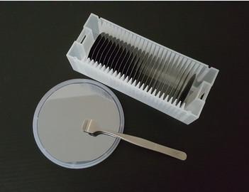
LDのための第一次/模造の等級のリン化インジウムのウエファーの厚さ350um
価格: by case
MOQ: 3pcs
納期: 1-4weeks
ブランド: zmkj
ハイライト:mgoの基質, ギャップのウエファー
2inch LDのためのNタイプのPタイプの厚さ350umの第一次等級の模造の等級のリン化インジウム水晶INP基質のウエファー
リン化インジウムの単結晶材料はリン化インジウムの基質(LD)の半導体レーザーのための主原料のほとんどの重要な半導体の混合物の1つ、発光ダイオード(LED)、光通信の生産のフォトディテクターです。それらの部品は、進水する情報受信機能を増幅する送信します。
リン化インジウムは、HEMTのように、高周波装置にとって等理想的HBTです。大きい特性のために、それは繊維光学コミュニケーション、マイクロウェーブ、太陽電池、ヘテロ接合のトランジスター、他の同じような先端技術... もっと見る
➤ 訪問 Webサイト

ゲルミウム基板 GE 平窓 光学レンズ 熱画像処理 紫外線スペクトロスコピー 高硬度
価格: Negotiable
MOQ: Negotiable
納期: 2-4 weeks
ブランド: ZMSH
ハイライト:熱イメージング 応用 ゲルマニウム基板, 赤外線スペクトロピー ゲルマニウム基板, 高硬度 ゲルマニウム基板
製品説明
ゲルマニウム基板 GE 平窓 光学レンズ 熱イメージング アプリケーションと赤外線スペクトロスコピー 高硬さ
ゲルマニウム窓 (Ge) は,2〜12μmの容認スペクトル範囲を持つ化学的に惰性物質で,高硬さ,良好な熱伝導性,一般的に使用される赤外線光学材料です.水に溶けない紫外線画像システムと赤外線スペクトロメーターシステムで使用されます.
窓は光学における基本的な光学要素の1つで,通常電子センサーや検出器の外環境への保護窓として使用されます.両側から環境を隔離するために使用されます計器の内側と外側を分離して,計器の内側と外側を隔離するように,内部部品を干渉から保護するため窓はシ... もっと見る
➤ 訪問 Webサイト
銅熱槽 基板 平底ピン型 高性能電子装置 Cu≥99.9%
価格: by case
MOQ: Negotiable
納期: 2-4weeks
ブランド: ZMSH
ハイライト:Cu≥99.9% 熱吸収基板, 高功率熱槽基板
c の要約上部熱槽基板
銅熱槽 基板 平底ピン型 高性能電子装置 Cu≥99.9%
コッパーヒートシンク基板は,高熱伝導性の純銅 (Cu≥99.9%) または銅合金 (C1100,C1020) 精密加工 (CNC切削) によるコア材料として, スタンプ,溶接,など). 主に高電力電子機器 (LED,IGBT,CPUなど) の熱管理に使用されます. 構造に応じて,フラットベースとピンフィンに分けることができます.異なる熱消耗要件に対応するように設計されたもの.
平底と針型の銅冷却基板
超高熱伝導性とカスタマイズ可能な構造により,銅冷却基板は高性能電子冷... もっと見る
➤ 訪問 Webサイト

インディアムアルセニード2インチ3インチ4インチ シングルクリスタル基板 N/Pタイプ 半導体
価格: Negotiable
MOQ: Negotiable
納期: 2-4 weeks
ブランド: ZMSH
ハイライト:4インチ インディウムアルセニド・ウェーファー, 3インチ インディウムアルセニド・ウェーファー, 2インチ インディウムアルセニド・ウェーバー
製品説明
インディアムアルセニード2インチ3インチ4インチ シングルクリスタル基板 N/Pタイプ 半導体
インディアム・インアス (Indium InAs) は,インディアムとアルセンからなる半導体.灰色の立方結晶の外観と942°Cの融点を有する.インディアムアルセニドは,波長範囲1〜3の赤外線検出器の構築に使用されます.8um.検出器は通常光電光二极管である.冷凍検出器は騒音が少ないが,室温での高電力アプリケーションにも使用できる.インディウムアルセニド は,二極電極レーザー の 製造 に も 用い られ ます.インディアムアルセニドは,ガリウムアルセニドに似ている直接帯隙材料である.イン... もっと見る
➤ 訪問 Webサイト
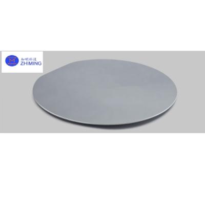
ゲルマニウム・ウェーファー半導体基板 <111> 集中光電CPV オーダーメイドサイズ形
価格: Negotiable
MOQ: Negotiable
納期: 2-4 weeks
ブランド: ZMSH
ハイライト:CPV ゲルマニアム・ウエフラー, オーダーメイドサイズ ゲルマニアム・ウェーファー, 半導体ゲルマニウムウエーファー
製品説明
ゲルマニアム・ウェーファー半導体基板 < 111> 集約光伏CPV オーダーメイドサイズ形
ゲルマニウムは半導体性能が良い.高純度ゲルマニウムは,P型ゲルマニウムの半導体を得るために,三価元素 (例えばインディウム,ガリウム,ボロン) とドーピングされる.半価元素 (e)N型ゲルマニウム半導体を得るためにドーピングされる.彼らは高い電子移動性と高い穴移動性を持っています.高品質のゲルマニウム基板は,濃縮光伏 (CPV) に使用できる宇宙の太陽光パネルや 高明度のLEDの用途
特徴
- 格子定数は,シリコンよりも大きいので,異質構造の構築に便利です.
- 高速電子装置... もっと見る
➤ 訪問 Webサイト
マグネシウム酸化物 純度 95% MgOフィルム 基板 5x5 10x10 20x20 厚さ 0.5mm 1.0mm 向き <001> <110> <111>
価格: by case
MOQ: 10pcs
納期: 1-4weeks
ブランド: zmkj
ハイライト:5×5 MgOフィルム基板, 20×20 MgOフィルム基板, 10×10 MgOフィルム基板
マグネシウムオキシド純度 95% MgOフィルム基板 5x5 10x10 20x20 厚さ 0.5mm 1.0mm 向き <001> <110> <111> 製品説明:
薄膜基板マグネシウムオキシド (MgO) 単結晶は高品質の基板材料で,高溶解点などの優れた物理的および化学的特性があります.低ダイレクトリ常数と損失高温超伝導性,鉄電性薄膜,磁性薄膜,その他の薄膜技術の製造に広く使用されています.優れた安定性と透明性により高品質の薄膜の成長に理想的な基盤を提供します.
特徴:
溶融点:マグネシウム酸化物単結晶は,高温で優れた安定性を示す,最大2800... もっと見る
➤ 訪問 Webサイト
InAsウエファードーピング Zn 2 インチ インディアムアルセニードウエファーDia 50mm 厚さ 500um <100> オーダーメイド
価格: Negotiable
MOQ: Negotiable
納期: 2-4 weeks
ブランド: ZMSH
ハイライト:パーソナライズされたインディウムアルセニド・ウェーファー, 2インチ インディウムアルセニド・ウェーバー, 500um インディウムアルセニド・ウェーファー
2インチインディアムアルセニード・ウェーファー インアス エピタキシャル・ウェーファー レーザーダイオード用InAsシングルクリスタルウェーファー 2インチ 3インチ 4インチ LDアプリケーションのためのInAs-Zn基板半導体ウエファー インディウムアルセニードレーザー エピタキシアルウエファー InAs-Znウエフルの特徴 - INA・ウエフルの製造に使用する- デザインアートワークでカスタマイズされたものをサポートしますレーザーで使われています レーザーで使われています- 1.5μmから5.6μmの波長範囲で,量子井戸構造- MOCVD や MBE,エッチング,金属化,包装などの技術を... もっと見る
➤ 訪問 Webサイト
DFB ウェーファー N-InP 基板 エピウェーファー 活性層 InGaAlAs/InGaAsP 2 4 6 インチ ガスのセンサー
価格: Negotiable
MOQ: Negotiable
納期: 2-4weeks
ブランド: ZMSH
ハイライト:2インチインP基板エピワファー, 4インチインP基板エピワファー, 6インチインプシストラートエピワファー
DFB ウェーファー N-InP 基板 エピウェーファー 活性層 InGaAlAs/InGaAsP 2 4 6 インチ ガスのセンサー
DFB ウェファーの N-InP 基板 エピウェファーの要約
n型インディアム・フォスフィード (N-InP) 基板の分散フィードバック (DFB) ウェーファーは,高性能DFBレーザー二極管の製造に使用される重要な材料である.このレーザーは,単モードを必要とするアプリケーションにとって不可欠です.,光通信,データ伝達,センシングなどの狭い線幅の光放出.DFBレーザーは通常1.3μmと1.55μm波長範囲で動作します.光ファイバーの低負荷伝送により光... もっと見る
➤ 訪問 Webサイト