310*320mm パネルサイズ パネルレベル QFN 低電気抵抗
価格: Negotiable
MOQ: Negotiable
納期: Negotiable
Description: 310*320mm panel size, Chip size: 0.76*0.61mm; Package size: 2.76*1.97mm; Package thickness: 360um, Application: Power management, Process introduction: The coming wafer is bumped with Cu post (e.g., 50 micro meters), after thining and dicing of wafer, chips with bump are picked and plac... もっと見る
➤ 訪問 Webサイト
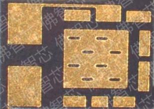
パネルレベル 梱包面 ダウンEWLB 高熱分散 高信頼性
価格: Negotiable
MOQ: Negotiable
納期: Negotiable
Description: 1,Compared with traditional packaging methods (e.g., wire bond and substrate), it has the obvious characteristics of high heat dissipation (thick Cu), high reliability (short connection and strong surface adhesion), high voltage and high current (thick Cu). 2,It can be used in various a... もっと見る
➤ 訪問 Webサイト
0.5mm 厚さ パネルレベル パッケージ パネルレベル BGA/CSP 電源アダプター用
価格: Negotiable
MOQ: Negotiable
納期: Negotiable
ブランド: FZX Fanout Process and Product
Description: 310*320mm panel size; Package size: 2.0*2.0mm; Package thickness: 0.5mm; Chip size: 1.0*1.6mm; Process type: FOPLP (Face Up); Process introduction: After the chip is picked and placed onto the temporary carrier board, the packaging process is carried out by compression molding, plasma c... もっと見る
➤ 訪問 Webサイト
パネルレベル パッケージ パネルレベル SiP 様々な産業で使用
価格: Negotiable
MOQ: Negotiable
納期: 1 month
ブランド: FZX Fanout Process and Product
Description: 310*320mm panel size; Advantage:Small SiP package size,such as 6*6mm/7.5*7.5mm;low power consumption;multi-chip packages, high assembly efficiency. Technical capability: different functional dies are assembled in one system,for example, MCU, Bluetooth and some passive chips are assemble... もっと見る
➤ 訪問 Webサイト
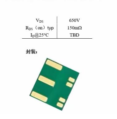
310*320mm パネルサイズ 薄型MOSチップ シリコン 低消費電力
価格: Negotiable
MOQ: 3000pcs
納期: 1 month
ブランド: FZX Fanout Process and Product
Description: Multi-chip MOSFET 310*320mm panel size; Package size: 2.0*2.0mm; Package thickness: 0.5mm; Chip size: 1.0*1.6mm; Process type: FOPLP (Face Up); Applications: Military applications, new energy vehicles, Power adapter, power amplifier, automotive electronics, etc. Competitive Advantage: 1... もっと見る
➤ 訪問 Webサイト
LEDチップ シリコン LED 常流ドライバーチップ 0.4mm*0.555mm*0.20mm
価格: Negotiable
MOQ: 3000pcs
納期: 1 month
ブランド: FZX Fanout Process and Product
Description: LED constant current driver chip; Chip size 0.4mm*0.555mm*0.20mm; Panel size 310*320mm; Package size 122mm*50mm; Process: Patch on the temporary carrier board, press EMC film, etching, then drill the hole, do electrode-plating. Applications: Mini-LED, lamps. Specifications: Chip size 0.... もっと見る
➤ 訪問 Webサイト
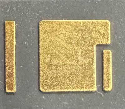
310*320mm ファンアウトパネルレベルパッケージング (FOPLP) 抵抗チップ ((シリコン)
価格: Negotiable
MOQ: 3000pcs
納期: 1 month
ブランド: FZX Fanout Process and Product
Description: Chip size: 0.76*0.61; 1.43 * 1.06; Package size: 2.76*1.97; 2.58 * 2.92; Package thickness: 360um; Process introduction: After the chip is reconstructed to the temporary carrier board, the pick and placement is performed and later plastic compressive molding, followed by grinding, laser... もっと見る
➤ 訪問 Webサイト
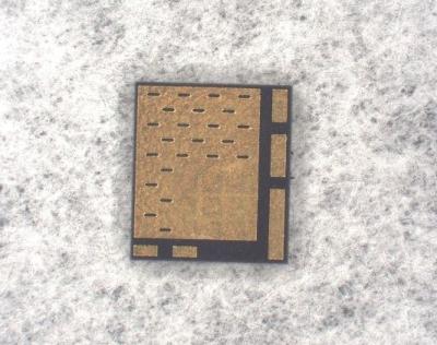
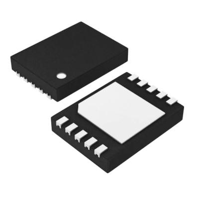
310*320mm ファンアウトパネルレベルパッケージ (FOPLP) ICチップ ((シリコン)
価格: Negotiable
MOQ: 3000pcs
納期: 1 month
ブランド: FZX Fanout Process and Product
Description: Panel size:310*320mm; Package size: 12*18*0.9mm; Package thickness: 0.9mm; Brief introduction to the process: After the temporary carrier board is attached, plastic sealing and chip reconstruction are done, the first layer of RDL is made, followed by etching +ABF pressing + laser drilli... もっと見る
➤ 訪問 Webサイト
310*320mm ファンアウトパネルレベルパッケージ (FOPLP) GaN製品
価格: Negotiable
MOQ: 3000pcs
納期: 1 month
ブランド: FZX Fanout Process and Product
310*320mm Panel size; DIE1 size:1.89*1.64mm; DIE2 size:0.926*0.626mm; Package size:6*7mm; Package thickness: 0.42mm; Process flow: The Face down packaging method is adopted for mounting, plastic sealing and grinding, the first layer of process is ABF pressing, and then etching and punching on the ba... もっと見る
➤ 訪問 Webサイト
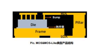
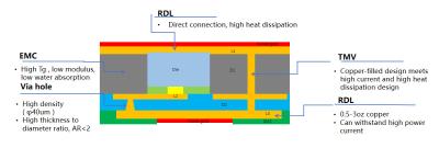
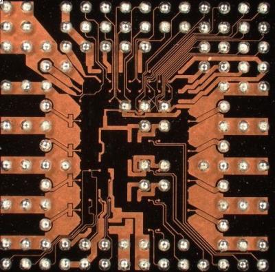
ファンアウトパネルレベルパッケージング (FOPLP) - 製品構造 (面向上) - ウェーファーバム
価格: Negotiable
MOQ: 3000pcs
納期: 1 month
ブランド: FZX Fan-Out Panel Level Packaging
Description: Die with bump of MOS&MOS-Like package can be picked and placed onto the temporary carrier; C mold is performed after above die placement with face-up methodology. The mold grinding, PVD and plating will be made for RDL. The TMV will be made for the top/bot layer connection. The surf... もっと見る
➤ 訪問 Webサイト
ファンアウトパネルレベルパッケージング (FOPLP) - 製品構造 (面向上) - ワイヤーボンドボール
価格: Negotiable
MOQ: 3000pcs
納期: 1 month
ブランド: FZX Fanout Process and Product
Description: As shown in above photo, compared with traditional packaging methods, the wire bond ball (copper or gold) can be made from wire bond process, it is similar to bump of chip, therefore, it has higher integration, high reliability, and low cost; through the FOPLP process , multiple MCU and... もっと見る
➤ 訪問 Webサイト
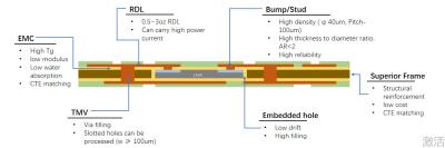
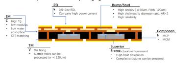
ファンアウトパネルレベルパッケージ (FOPLP) 製品構造 組み込みパッケージ
価格: Negotiable
MOQ: 3000pcs
納期: 1 month
ブランド: FZX
Description: 1,Compared with traditional packaging methods, this advanced packaging replaces wire bond and substrate, therefore, it has demonstrated the characteristic of higher integration, high reliability, and low cost ; 2,While maintaining the original foot position design, it is much thinner an... もっと見る
➤ 訪問 Webサイト
310*320mm ファンアウトパネルレベルパッケージング (FOPLP) ラジオ周波数 (RF)
価格: Negotiable
MOQ: 3000pcs
納期: 1 month
ブランド: FZX Fanout Process and Product
Description: Panel size:310*320mm Package size: 7*6mm Package thickness: 0.75mm Process flow: The Face down packaging method is adopted for mounting, plastic sealing and grinding, the first layer of process is ABF pressing, and then etching and punching on the back of the plastic sealing material, t... もっと見る
➤ 訪問 Webサイト
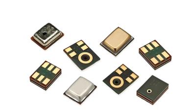
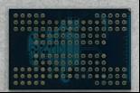
310*320mm 扇風機パネルレベルパッケージ (FOPLP) MEMS マイクロフォンパッケージ
価格: Negotiable
MOQ: 3000pcs
納期: 1 month
ブランド: FZX Fanout Process and Product
Description: Plating uniformity: ≤10%; Package size: 3*2mm; Package thickness: 0.26mm; Chip size: 0.96*0.78mm; Process type: FOPLP (310X320mm); Applications: Mobile phone, Bluetooth headset,MEMS, wearable electronics. Specifications: Package size: 3*2mm; Package thickness: 0.26mm; Chip size: 0.96*0.... もっと見る
➤ 訪問 Webサイト
310*320mmファンアウトパネルレベルパッケージ (FOPLP) CPO/ミニ/マイクロLED
価格: Negotiable
MOQ: 3000pcs
納期: 1 month
ブランド: FZX Fanout Process and Product
Description: LED constant current driver chip; Chip size 0.4mm*0.555mm*0.20mm; Panel size 310*320mm; Package size 122mm*50mm; Process: Patch on the temporary carrier board, press EMC film, etching, then drill the hole, do electrode-plating. Applications: Mini-LED, lamps Specifications: Chip size 0.4... もっと見る
➤ 訪問 Webサイト
310*320mm 扇風機パネルレベルパッケージ (FOPLP) パワーパック
価格: Negotiable
MOQ: 3000pcs
納期: 1 month
ブランド: FZX Fanout Process and Product
Description: 310*320mm panel size; Package size: 2.0*2.0mm; Package thickness: 0.5mm; Chip size: 1.0*1.6mm; Process type: FOPLP (Face Up); Process flow: face up encapsulation method is adopted. After a single patch, bump, plastic sealing and grinding (exposing the ball), then punch holes and electro... もっと見る
➤ 訪問 Webサイト
高画質比 TGV 半導体包装のための鋳造能力
価格: Negotiable
MOQ: 10 panel
納期: 1 month
ブランド: FZX -TGV
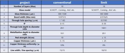
Description: As shown in the following table, the glass core substrate with 510mmX515mm size can be manufactured inside the manufacturing line. The glass thickness is varied from 0.3mm to 1.5mm (some can be extended to 5mm thick). The aspect ratio (diameter/ thickness of glass)can be varied from 1:1... もっと見る
➤ 訪問 Webサイト

高効率なガラス35umの穴/盲目穴はGPU/CPU/AIチップのために
価格: Negotiable
MOQ: 10 panel
納期: 1 month
ブランド: FZX Fanout Process and Product
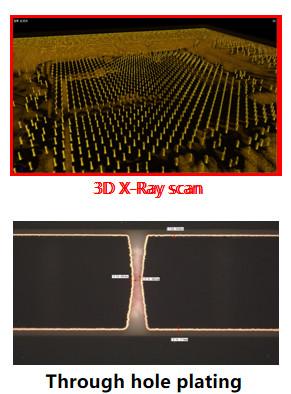
Description: As shown below photo, the blind or through holes can be made with angle controlling, the laser and acid methodology can be combined together to make customer specific holes. The glass can be coming from different suppliers, e.g., AF32/BF33 (Schott), EAGLE XG or AGC, etc. The shape of ho... もっと見る
➤ 訪問 Webサイト
高効率ガラス基板 サイズ 510*515mm PVD 300mm-600mm
価格: Negotiable
MOQ: 10 panel
納期: 1 month
ブランド: FZX Fanout Process and Product
Description: The panel level PVD can be performed at both sides of the panel simultaneously. It is high efficient and time saving process. The panel sizes are varied within 300mm-600mm. Ti/Cu can be performed as the seed layers. The thickness is controlled with 0.1-2 micro meters. The uniformity in ... もっと見る
➤ 訪問 Webサイト
ガラスの基板技術 - 双面塗装 安定し,簡単に維持
価格: Negotiable
MOQ: 10 panel
納期: 1 month
ブランド: FZX -plating
Description: The panel plating machine is used for plating, Plating uniformity can achieve below 10%,High aspect ratio of glass through-hole plating can be performed, AR < 10 : 1 1,All pass padding Dia .: 100 μm Cu thick .: 10 μm Glass thick .: 600μm 2,Through hole plating Dia .: 50 μm Cu thick .... もっと見る
➤ 訪問 Webサイト